
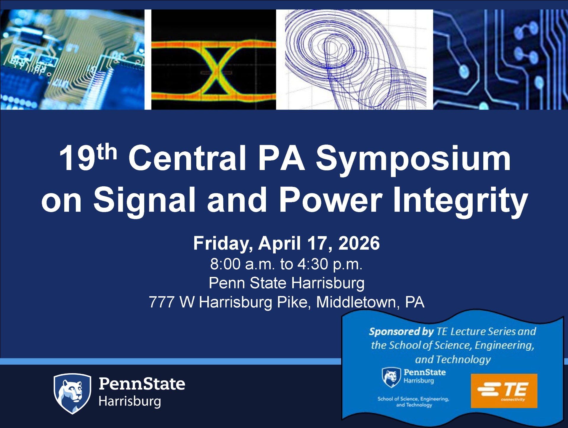
19th Central PA Symposium of Signal Integrity and Power Integrity, Penn State Harrisburg April 17, 2026
19th Central PA Symposium on Signal and Power Integrity
Sponsored by TE Lectures Series and Penn State Harrisburg
Friday, April 17 from 8:00 a.m. to 4:30 p.m.
Venue: Penn State Harrisburg
Registration: https://web.cvent.com/event/e1894308-23a3-4c74-a58b-8104b360707d/summary
PROGRAM:
Registration and Breakfast | ||
Welcoming Remarks Plenary Speaker 1, Capital Union Building (CUB), Convocation Room Title: "Crosstalk Sensitivity New Finding on PCIe 7.0 Channel Through S-Parameter Manipulation" Mr. Quresh Bohra, System Architect, TE Connectivity Abstract: The study offers insights into frequency-dependent crosstalk behaviors critical for designing and selecting PCIe 7.0 connectors. It contributes to the development of the PCIe 7.0 ecosystem by providing valuable information on crosstalk management and component selection for improved channel optimization, ultimately supporting the continued evolution of PCIe technology. | ||
Workshop 1 CUB Convocation room Rohde & Schwarz | Workshop 2, EAB 110 Keysight | |
Plenary Speaker 2, CUB Title: “Machine Learning for EDA: Learning Algorithms for Analog and RF Physical Design” Dr. Ioannis Savidis, Director, Integrated Circuits and Electronics (ICE) Design & Analysis Laboratory, Department of Electrical and Computer Engineering, Drexel University, Abstract: In the ever-evolving landscape of Electronic Design Automation (EDA), the integration of Artificial Intelligence (AI) and Machine Learning (ML) algorithms with traditional heuristic optimization algorithms has emerged as a transformative force in automated circuit design. Machine learning, including deep learning, has the potential to significantly improve theaccuracy, speed, efficiency, and reliability of EDA tasks such as circuit modeling, simulation, layout design, and optimization. This presentation delves into the dynamic intersection of AI/ML and EDA, exploring state-of-the-art techniques shaping the analog and RF physical design space. Delving into such cutting-edge advancements, I will describe current AI/ML research performed by the Drexel ICE Lab that extends beyond traditional analog and RF design paradigms, with the goal of enabling designers to navigate complexities with unparalleled efficiency and accuracy. Specifically, a focus on state-of-the-art learning and optimization techniques for the modeling and design of analog and RF ICs will be presented and described. Practical considerations, challenges, and opportunities of ML algorithms for analog and RF circuit design will be discussed, with a focus on the use of such algorithms for prediction and optimization tasks within the EDA design flow. | ||
Lunch | ||
Plenary Speaker 3. CUB Title: Signal and Power Integrity Challenges in Industrial Single Pair Ethernet Practical Measurement, Emulation, and Automated Validation Ms. Palak Patel, Telebyte, and Mr. Arnold Offner Phoenix Contact Ms. Patel is the Technical Product Manager – SPE Testing Solutions, Telebyte Inc and , Charotar University of Science and Technology (CHARUSAT), Anand, India Mr. Arnold Offner is a Product Marketing Manager, Phoenix Contact USA. Abstract: The industry need for single pair carrying both power and ethernet data has been known for quite a while. The IEEE 802.3cg standard published in 2022, and the pending IEEE 802.3dg standard promise to take ethernet connectivity all the way to the device edge. This presentation examines practical SI/PI failure mechanisms observed in industrial SPE/APL systems and describes automated physical-layer test methodologies used to uncover them. The talk also highlights the role of fully automated test platforms in reducing setup variability, expanding test coverage, and enabling unattended operation across development, compliance, and interoperability workflows. | ||
Plenary Speaker 4, CUB Talk Title: Physics Driven Paths to Scalable Accelerator Fabrics Andrew D. Josephson , Samtec Abstract: As signaling rates approach 400 Gb/s per lane, interconnect design enters a regime where electromagnetic wavelengths collapse into package and PCB geometries. In this regime, signal‑integrity limits are dominated not by smooth insertion loss, but by wavelength‑scale resonance, cavity excitation, and unintended radiation. These effects create fundamental brick walls that constrain traditional PCB‑centric and front‑panel channel architectures, independent of SerDes capability. This talk reviews the physical mechanisms behind these brick walls and explains why they force a shift toward shorter‑reach, topology‑aware interconnect strategies. Chip‑to‑chip (C2C) and co‑packaged copper links are presented as architectural responses driven by geometry and reach, supported by C2C copper twinax channels demonstrating clean wide‑bandwidth behavior. The discussion then expands to system design, introducing a hardware‑centric, IO‑normalized bisection bandwidth metric to show how interconnect mesh topologies effect compute cluster bandwidth performance for Ai-scale workloads. Author Biography: Andrew D. Josephson is a Signal Integrity (SI) Technologist at Samtec, where he focuses on emerging data rate technology development, maturation, and standardization. His work centers on the physical limits of copper interconnects, packaging, and connector systems supporting next‑generation computing and networking platforms. Andrew is a contributor to IEEE and OIF 400G pathfinding efforts in industry and an author of numerous technical publications addressing signal integrity and architectural challenges at data rates beyond 200 Gb/s per lane. Andrew holds a Bachelor of Science in Electrical Engineering from the University of Minnesota | ||
Plenary Speaker 5, CUB Title: “PocketFabs: A New Paradigm for Right-Sized, Modular, and Distributed Semiconductor Manufacturing Systems” Dr. Marcelo Zuffo, University of Sao Paulo, Brazil (top EE School worldwide) Traditional semiconductor fabrication relies on highly standardized, large-scale manufacturing processes to produce integrated circuits (ICs) in industrial fabrication facilities. Optimized for high volume, high yield, and extreme precision, these processes form the backbone of modern microelectronics. Achieving such performance, however, requires substantial capital expenditure and a highly skilled workforce, resulting in a strong concentration of fabrication capabilities in so-called megafabs, each requiring investments of several billion dollars. In recent years, the strategic importance of semiconductors to the global economy has intensified, exposing vulnerabilities in global supply chains and elevating semiconductor manufacturing to a central issue in international competition and geopolitical tensions. These challenges have stimulated growing interest in alternative manufacturing paradigms, including sustainable, distributed, and modular fabrication models. In this talk, we introduce the Semiconductor PocketFab concept, a novel approach to enhance flexibility, resilience, and accessibility in semiconductor manufacturing. PocketFab proposes a significant downsizing of conventional fabrication facilities, enabling an ultra-compact, right-sized, fully automated, human-less, end-to-end semiconductor manufacturing pipeline. The architecture is designed to support localized and flexible production while substantially reducing energy consumption, water usage, and cleanroom footprint compared to traditional fabs. The concept further incorporates key Industry 4.0 principles, including modular automation, system interoperability, data-driven process control, and digitally integrated production systems. Guided by this concept, we implemented a 3D chiplet heterogeneous packaging PocketFab as a practical instantiation of the proposed architecture. Dr. Marcelo Knörich Zuffo, IEEE Senior Member, is a Full Professor of Electronic Systems Engineering at the University of São Paulo (USP) and a leading figure in Brazil’s digital and semiconductor innovation landscape. He leads the Interactive Electronics Group at the Laboratory for Integrated Systems (LSI), driving research at the intersection of virtual reality, digital health, AIoT, embedded systems, and large-scale interactive infrastructures. A pioneer of immersive and digital technologies in Latin America, he led the implementation of the region’s first CAVE (Cave Automatic Virtual Environment) system and played a central role in the development of the Brazilian Digital TV System, now adopted across most of the continent. | ||
Workshop 4 (CUB) Title: Accelerate your design cycle: What you need to know about HVM tradeoffs Scotty Neally is a seasoned Signal Integrity expert with over 15 years of experience driving innovation for component and system level SerDes and Memory design. | Workshop 5 EAB 110 Title: Optimizing EMI Performance for Unmanned Aerial Vehicle (UAV) Printed Circuit Board Dr. Kapil Sharma, Assistant Professor of Electrical Engineering, University of Alaska, Fairbanks | |